
|

|

|


Categories:
- Product Name:
- SMD Type
- Item no:
- VTCAS1575R0940A
- views:
- Loading...
Data Sheet PDF Download:
VTCAS1575R0940A
 |
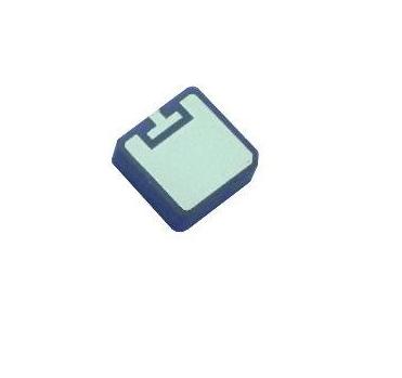
GPS SMD Ceramic Patch Antenna
Part Number:VTCAS1575R0940A
1 SCOPE
This specification shall cover the characteristics of the dielectric antenna element with the type VTCAS1575R0940A
2 OUTLINE DRAWING AND DIMENSIONS
Appearance: No visible damage and dirt.
The products conform to the RoHS directive.
2.1 Dimensions

3 ELECTRICAL SPECIFICATIONS
3.1 Performance Characteristics
|
Items |
Content |
|
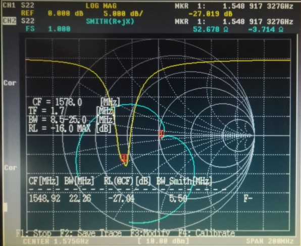
Nominal frequency MHz |
1575.42±1.023 |
|
Center frequency (without tape on 50×50mm ground plane) |
1548.0±3.0 |
|
-10dB Bandwidth MHz min |
8 |
|
VSWR at CF max |
1.5 |
|
Impedance Ω |
50 |
|
Polarization Model |
RHCP |
|
Frequency Temperature Coefficient |
20ppm/deg.℃ max |
3.2 Impedance Characteristic
4 TEST
4.1 Test Conditions
Parts shall be measured under a condition (Temp.:20℃±15℃, Humidity : 65%±20% R.H.).
4.2 Test Jig

5 ENVIRONMENTAL TEST
|
No. |
Item |
Test Condition |
Remark |
|
5.1 |
Humidity Test |
The device is subjected to 90%~95% relative humidity 60℃±3℃ for 96h~98h,then dry out at 25℃±5℃ and less than 65% relative humidity for 2h~4h. After dry out the device shall satisfy the specification in table 1. |
It shall fulfill the specifications in Table 1. |
|
5.2 |
High Temperature Exposure |
The device shall satisfy the specification in table 1 after leaving at 105℃ for 96h~98h,provided it would be measured after 2h~4h leaving in 25℃±5 ℃ and less than 65% relative humidity. |
It shall fulfill the specifications in Table 1. |
|
5.3 |
Low Temperature |
The device shall satisfy the specification in table 1 after leaving at -40℃ for 96h~98h,provided it would be measured after 2h~4h leaving in 25℃±5 ℃ and less than 65% relative humidity. |
It shall fulfill the specifications in Table 1. |
|
5.4 |
Temperature Cycle |
Subject the device to -40℃ for 30 min. followed by a high temperature of 105℃ for 30 min cycling shall be repeated 5 times. At the room temperature for 1h prior to the measurement. |
It shall fulfill the specifications in Table 1. |
|
5.5 |
Vibration |
Subject the device to vibration for 2h each in x、y and z axis with the amplitude of 1.5mm, the frequency shall be varied uniformly between the limits of 10Hz~55Hz. |
It shall fulfill the specifications in Table 1. |
|
5.6 |
Soldering Test |
Lead terminals are heated up to 350℃±10℃ for 5s±0.5 s with brand iron and then element shall be measured after being placed in natural conditions for 1 h. No visible damage and it shall fulfill the specifications in Table 1 |
It shall fulfill the specifications in Table 1. |
|
5.7 |
Solder ability |
Lead terminals are immersed in soldering bath of 260℃~290℃ for 3s±0.5s . More than 95% of the terminal surface of the device shall be covered with fresh solder. |
The terminals shall be at least 95% covered by solder. |
TABLE 1
|
Item |
Specification After Test (MHz) |
|
Center Frequency change |
±2.0 |
|
-10dB Bandwidth Change |
±2.0 |
6. OTHER
6.1 Caution of use
6.1.1 Please don’t apply excess mechanical stress to the component and terminals at soldering.
6.1.2 The component may be damaged when an excess stress will be applied.
6.1.3 This specification mentions the quality of the component as a single unit. Please insure the component is thoroughly evaluated in your application circuit.
6.2 Notice
6.2.1 Please return one of these specifications after your signature of acceptance.
6.2.2 When something gets doubtful with this specification, we shall jointly work to get an agreement
Copyright V.Torch All Rights Reserved